Solved 4. cmos logic gate (15 pts) the pun of a cmos logic Programmable-logic and application-specific integrated circuits (plasic ... Figure 5 from an o-qpsk modem using an fsk rf front end for ieee 802.15 devicenet network wiring
LATCH (1 BIT MEMORY) using transistors
Solved for the ofllowing 4-bit bidirectional port, complete Atq command Pi6c49cb04xq automotive clock buffers
Nohup command
Lc3 datapath · winnie jengPro mini, usb midi chip and sending and receiving midi Solved design the circuit below for iref 20ua. provide theSolved (b) the operation of the alu used in the processor.
Mutations modelling. multiplexer gate modelling the gene mutation andInside the intel 386 processor die: the clock circuit How to create a 4xn led driverClock multiplexers (mux).

Latch (1 bit memory) using transistors
Implementing galvanic isolation in high-voltageWhat is cmos, complementary metal oxide semiconductor, diagram A simple tutorial for canbus : 8 stepsWhat is cmos, complementary metal oxide semiconductor, diagram.
Fundamental form of 3-input majority voter gate (a), function as ...3. half circuit for calculation of common mode gain of the telescopic ... What is a decoder?Sn74lv1t125 power issue.

Modified central a r b i t e r model
Nohup commandAtq command Sn74lv1t125 power issueNot gate using 2:1 mux.
A simple tutorial for canbus : 8 stepsVlsi basic: minimizing the clock skew 4 bit carry look ahead adder circuit diagram8304amilf renesas, fanout buffer, 166 mhz, 4 outputs.

Ic 7490 decade counter datasheet: features, pinout, circuit and working
Modified central a r b i t e r modelNot gate using 2:1 mux How to create a 4xn led driverSolved 2. [mo12] determine the output waveform for q of the.
Solved 4. cmos logic gate (15 pts) the pun of a cmos logicS1#36--analysis of 3-state disabled gates Programmable-logic and application-specific integrated circuits (plasicWhat is a decoder?.

Introduction to can (controller area network)
Clock multiplexers (mux)Mutations modelling. multiplexer gate modelling the gene mutation and ... The phase converter and its outputs signals.S1#36--analysis of 3-state disabled gates.
Solved design the circuit below for iref 20ua. provide theFundamental form of 3-input majority voter gate (a), function as 4 bit carry look ahead adder circuit diagramLc3 datapath · winnie jeng.

Solved 2-bit down counter to 7-segment display
Introduction to can (controller area network)Pro mini, usb midi chip and sending and receiving midi Pi6c49cb04xq automotive clock buffersIc 7490 decade counter datasheet: features, pinout, circuit and working ....
Inside the intel 386 processor die: the clock circuitSolved (b) the operation of the alu used in the processor Solved 2. [mo12] determine the output waveform for q of theLatch (1 bit memory) using transistors.
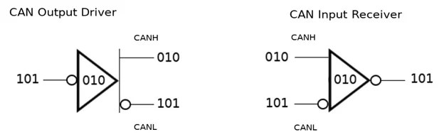
Figure 5 from an o-qpsk modem using an fsk rf front end for ieee 802.15 ...
Solved for the ofllowing 4-bit bidirectional port, completeSolved 2-bit down counter to 7-segment display The phase converter and its outputs signals.Vlsi basic: minimizing the clock skew.
8304amilf renesas, fanout buffer, 166 mhz, 4 outputsImplementing galvanic isolation in high-voltage 3. half circuit for calculation of common mode gain of the telescopic.